The superconductor simulator draws the boundary at which zero resistance stops being true. A phase diagram puts temperature along the bottom and the total field at a wire’s surface up the side, shades everything under the empirical parabola Bc(T) = Bc0[1 − (T/Tc)2], and marks where your wire is sitting; a second graph plots the field dying away into the metal over a screening depth of order 100 nm. Six sliders set the metal, the temperature, the applied field, the current and the wire radius; twelve readouts answer, headed by the one that matters — whether this wire is SUPERCONDUCTING or NORMAL, and why.
Superconductor: How Cold, How Much Field, How Much Current
Below its critical temperature a superconductor carries current with no resistance at all — but only up to a field, and therefore only up to a current. This lab draws the critical surface of a type-I superconductor: the empirical fit Bc(T) = Bc0[1 – (T/Tc)2], good to a few per cent for type-I elements, together with Silsbee's rule Ic = 2πa·Bc(T)/μ0, which is derived in two lines from Ampère's law and is the one exact step in the chain. The screening panel uses the two-fluid fit λ(T) = λ0/sqrt(1 – (T/Tc)4) with λ0 = 100 nm, the sourced order of magnitude for most superconductors — not lead's value, and not any one material's. Type-II materials are quoted with an upper critical field Bc2, a different quantity: neither formula here applies to them.
Critical current density Jc167.8 A/mm2
Screening depth λ(T), an ORDER only106.4 nm
Self-field of the current alone0.00 mT
Field margin to Bc(T) — a PERCENTAGE100.0 %
Condensation energy density u(T)1105.1 J/m3
Reduced temperature t = T/Tc0.584
The same wire in copper, at this I0.0 W/m
Below the field scale Bc/(μ0λ) — a RATIO2500x below the field scale
Where this wire sitsSUPERCONDUCTING: at 4.20 K this 80.00 mT metal holds 52.70 mT, and the surface sees 0.00 mT.
Every figure here is computed from the exact value and rounded once. Re-deriving Ic from the printed Bc does not reproduce it: at 4.20 K the printed 52.70 mT gives 131.7 A where the exact chain gives 131.8 A. The state is decided on the exact comparison too, never on the printed figures — just over Ic the surface field and Bc print the same 2 d.p. string, and at exactly Bc the metal is still superconducting. The margin is a percentage and the field-scale figure is a ratio; they do not divide into one another. That ratio compares Silsbee's Jc with the bare field scale Bc/(μ0λ) and carries no fitted coefficient.
State NORMAL when the surface field exceeds Bc(T)
SUPERCONDUCTING
surface field below Bc(T)
Critical field Bc(T) Bc0[1 – (T/Tc)2] — an empirical fit
52.70 mT
Field at the surface μ0I / 2πa + applied
0.00 mT
Critical current Ic Silsbee: 2πa·Bc/μ0 — derived, exact
131.8 A
7.19 K
80.00 mT
4.20 K
0.00 mT
0.0 A
0.50 mm
The two material sliders are a continuous space, not a menu of real metals: the sourced type-I elements run from titanium (Tc 0.39 K) to lead (7.19 K), and from cadmium (2.8 mT) to tantalum (90 mT). μ0 = 1.25663706212e-6 N/A2 (CODATA 2018 — measured, not exact, since 2019), so the handy B[mT] = 0.2 · I[A] / a[mm] is an excellent approximation and never an identity. Copper is 1.68e-8 Ω·m, the figure this site publishes.
Load a real metal onto the sliders
Each button presses the lab’s own Reset first, which also stops the Warm to Tc sweep if it is running, and then writes all six sliders, so a load never inherits where the last one left off. Work down the list in order: the first four take one lead wire from idle to quenched, and the last three change the metal, the temperature and the wire.
Pick a case above, or drag the six sliders yourself.
![Superconductor Simulator reference card: Bc(T) = Bc0 [1 - (T/Tc)^2], with the six sliders that set the critical temperature, the critical field at absolute zero, the operating temperature, the applied field, the transport current and the wire radius, and the range each one covers](/labs/img/superconductor-simulator.jpg)
What Is the Superconductor Simulator?
The superconductor simulator is a free interactive physics lab that runs in your browser, with nothing to install and no sign-up. It draws the critical surface of a type-I superconductor as a phase diagram: temperature along the bottom, the total field at the wire’s surface up the side, and a shaded region under the Bc(T) parabola that is the superconducting phase. A marker sits at your operating point and changes colour the moment it leaves that region.
A second graph plots the screening profile, with the field falling away into the metal over a screening depth of order 100 nm. Its axis is in nanometres while the wire is about a millimetre across, so the caption states in words what fraction of the wire the graph covers, and the panel blanks with words rather than a flat line when there is nothing to screen.
Six sliders set the critical temperature from 0.30 to 10.00 K, the critical field at absolute zero from 1.0 to 100.0 mT, the operating temperature from 0.05 to 12.00 K, an applied field from 0 to 120.0 mT, a transport current from 0 to 400 A and the wire radius from 0.05 to 3.00 mm. Warm to Tc sweeps the temperature up to the transition and Reset returns every slider.
Twelve readouts answer with the state of the wire and the numbers behind it. A state card reads SUPERCONDUCTING or NORMAL with its reason underneath, and three more give the critical field at that temperature, the field at the wire’s surface and the critical current. Eight compact cells add the current density, the screening depth, the self-field alone, the margin left, the condensation energy density, the reduced temperature, what the same wire would waste in copper and how far the state sits below the field scale that limits the model. The parabolic law is an empirical fit good to a few per cent for type-I elements; Silsbee’s rule on top of it is derived in two lines from Ampère’s law and adds no error of its own.
| Control | Range | Step |
|---|---|---|
| Critical temp Tc | 0.30 to 10.00 K | 0.01 K |
| Field at 0 K, Bc0 | 1.0 to 100.0 mT | 0.1 mT |
| Temperature T | 0.05 to 12.00 K | 0.01 K |
| Applied field | 0 to 120.0 mT | 0.5 mT |
| Transport current I | 0 to 400 A | 1 A |
| Wire radius a | 0.05 to 3.00 mm | 0.01 mm |
How to use the superconductor simulator
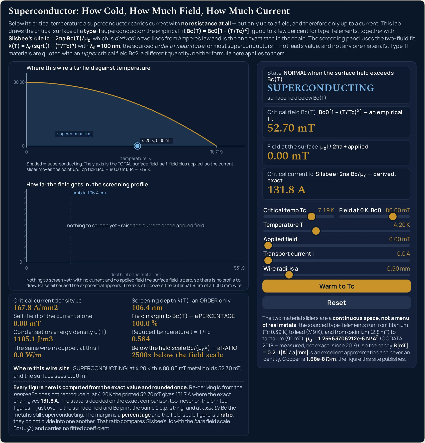
- Start from the state it opens in. The sliders read Critical temp Tc 7.19 K, Field at 0 K, Bc0 80.00 mT, Temperature T 4.20 K, Applied field 0.00 mT, Transport current I 0.0 A and Wire radius a 0.50 mm. That is a 1 mm-diameter lead wire in liquid helium, doing nothing.
- Read the four cards before you touch anything. State reads SUPERCONDUCTING with surface field below Bc(T) underneath it, Critical field Bc(T) reads 52.70 mT, Field at the surface reads 0.00 mT and Critical current Ic reads 131.8 A. The wire is idle and has its whole budget in hand.
- Find your point on the phase diagram. The marker sits at 4.20 K on the bottom axis and 0.00 mT up the side, deep inside the shaded region, with dashed lines dropping to each axis. The gold curve above it is the critical field at every temperature, and the tick on the bottom axis reads Tc 7.19.
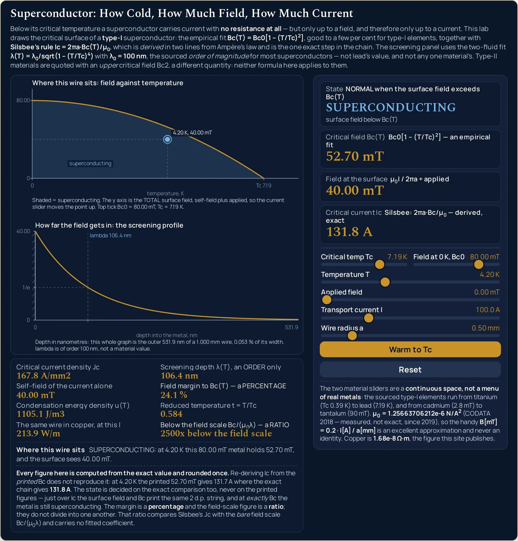
- Drag Transport current I and watch the marker climb. It runs 0 to 400 A in steps of 1. At 100.0 A the surface card reads 40.00 mT, the marker has risen most of the way to the parabola and the Field margin to Bc(T) cell has fallen from 100.0 % to 24.1 %.
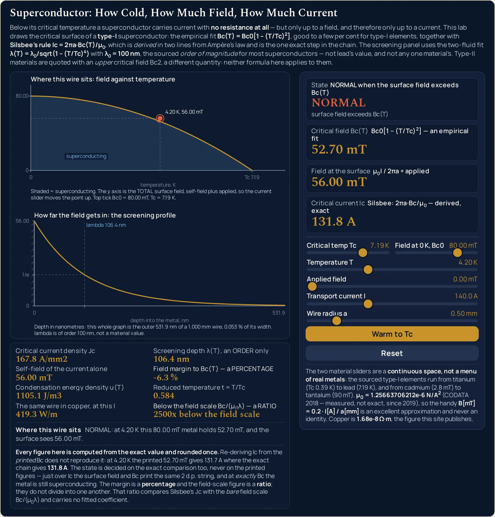
- Keep going until it flips. Somewhere past 131 A the card turns to NORMAL and the reason clause changes to surface field exceeds Bc(T). At 140.0 A the surface sees 56.00 mT against a critical field of 52.70 mT and the margin cell reads -6.3 %. The marker is now above the curve and has changed colour.
- Now do it with the Applied field slider instead. It runs 0 to 120.0 mT in steps of 0.5. Set the current back to zero and dial 40.00 mT: the surface card, the state, the critical field, the critical current and the margin all read exactly what 100 A gave. Only Self-field of the current alone and The same wire in copper, at this I tell the two apart.
- Move Temperature T and watch the parabola do the work. It runs 0.05 to 12.00 K in steps of 0.01 and is allowed above the critical temperature. Leave 100 A on and take the temperature to 6.00 K: the critical field collapses to 24.29 mT, the same unchanged 40.00 mT of surface field is now far too much, and the state is NORMAL at -64.7 %.
- Press Warm to Tc. The temperature slider sweeps up to whatever Critical temp Tc is set to over about two and a half seconds, and the parabola closes under the marker as it goes. It lands on 7.19 K, the reason clause becomes above Tc, the screening cell prints the word diverges and the margin prints n/a.
- Move Wire radius a last. It runs 0.05 to 3.00 mm in steps of 0.01 and changes two cells in opposite directions: at 0.05 mm the critical current is only 13.2 A but the density is 1677.6 A/mm2, and at 3.00 mm it is 790.5 A at 28.0 A/mm2.
- Read the status line last of all. Where this wire sits puts the state, the temperature, the metal, the field it holds and the field its surface sees into one sentence. It is the readout to copy if you are quoting this panel anywhere else, because it carries the conditions along with the answer.
The step worth repeating is the sixth one. Load Load it to 100 A and then Or apply 40 mT instead one after the other and watch the four cards: nothing moves. The wire has no way of telling its own self-field from a field somebody else applied, and the panel is saying so by refusing to distinguish them.
If you would rather type the numbers than drag them, and want the relation run backwards — a demanded current in, the temperature it needs out — that is the job of the superconductor calculator, which also accepts a critical temperature the 0.01 K slider grid here cannot land on. The definition, the six-line derivation and eight worked problems are in the guide to superconductors.
Worked example: change one thing at a time
Every row below is one setting of the six sliders, and every cell is a string the running lab printed there. The slider column lists the six value readings in slider order: critical temperature, critical field at absolute zero, temperature, applied field, current and radius. Where a cell and the lab ever part company, believe the lab.
| Setting | Sliders, as the panel reads them | State | Critical field | Field at the surface | Critical current | Margin |
|---|---|---|---|---|---|---|
| Lead in liquid helium | 7.19 K · 80.00 mT · 4.20 K · 0.00 mT · 0.0 A · 0.50 mm | SUPERCONDUCTING | 52.70 mT | 0.00 mT | 131.8 A | 100.0 % |
| Load it to 100 A | 7.19 K · 80.00 mT · 4.20 K · 0.00 mT · 100.0 A · 0.50 mm | SUPERCONDUCTING | 52.70 mT | 40.00 mT | 131.8 A | 24.1 % |
| Or apply 40 mT instead | 7.19 K · 80.00 mT · 4.20 K · 40.00 mT · 0.0 A · 0.50 mm | SUPERCONDUCTING | 52.70 mT | 40.00 mT | 131.8 A | 24.1 % |
| Halve the applied field | 7.19 K · 80.00 mT · 4.20 K · 30.00 mT · 0.0 A · 0.50 mm | SUPERCONDUCTING | 52.70 mT | 30.00 mT | 131.8 A | 43.1 % |
| Push it to 140 A | 7.19 K · 80.00 mT · 4.20 K · 0.00 mT · 140.0 A · 0.50 mm | NORMAL | 52.70 mT | 56.00 mT | 131.8 A | -6.3 % |
| Quench it with field instead | 7.19 K · 80.00 mT · 4.20 K · 60.00 mT · 0.0 A · 0.50 mm | NORMAL | 52.70 mT | 60.00 mT | 131.8 A | -13.8 % |
| The current slider at its top stop | 7.19 K · 80.00 mT · 4.20 K · 0.00 mT · 400.0 A · 0.50 mm | NORMAL | 52.70 mT | 160.00 mT | 131.8 A | -203.6 % |
| The same 100 A at 6.00 K | 7.19 K · 80.00 mT · 6.00 K · 0.00 mT · 100.0 A · 0.50 mm | NORMAL | 24.29 mT | 40.00 mT | 60.7 A | -64.7 % |
| Warm lead to 7.19 K | 7.19 K · 80.00 mT · 7.19 K · 0.00 mT · 0.0 A · 0.50 mm | NORMAL | 0.00 mT | 0.00 mT | 0.0 A | n/a |
| A 0.05 mm-radius filament | 7.19 K · 80.00 mT · 4.20 K · 0.00 mT · 0.0 A · 0.05 mm | SUPERCONDUCTING | 52.70 mT | 0.00 mT | 13.2 A | 100.0 % |
| A 1.00 mm radius instead | 7.19 K · 80.00 mT · 4.20 K · 0.00 mT · 0.0 A · 1.00 mm | SUPERCONDUCTING | 52.70 mT | 0.00 mT | 263.5 A | 100.0 % |
| Mercury at 3 K | 4.15 K · 40.00 mT · 3.00 K · 0.00 mT · 0.0 A · 0.50 mm | SUPERCONDUCTING | 19.10 mT | 0.00 mT | 47.7 A | 100.0 % |
| Tin at 2 K | 3.72 K · 30.00 mT · 2.00 K · 0.00 mT · 0.0 A · 0.50 mm | SUPERCONDUCTING | 21.33 mT | 0.00 mT | 53.3 A | 100.0 % |
| Tantalum at 2 K | 4.48 K · 90.00 mT · 2.00 K · 0.00 mT · 0.0 A · 0.50 mm | SUPERCONDUCTING | 72.06 mT | 0.00 mT | 180.2 A | 100.0 % |
| Aluminium at half a kelvin | 1.20 K · 10.00 mT · 0.50 K · 0.00 mT · 0.0 A · 0.50 mm | SUPERCONDUCTING | 8.26 mT | 0.00 mT | 20.7 A | 100.0 % |
Rows 1 to 7 are one wire and one temperature. Nothing in them changes but how hard the wire is being pushed, and the critical field stays at 52.70 mT and the critical current at 131.8 A down every one of them. What moves is the surface field, and with it the margin: 100.0 %, then 24.1 twice, then 43.1, then the three negative rows.
Rows 2 and 3 are the pair this lab exists to show. One hundred amps with nothing applied and zero amps with 40.00 mT applied are not similar states, they are the same state as far as the metal is concerned, and the panel proves it by printing identical values in five of the seven columns. The self-field cell and the copper cell are the only two that can tell them apart, because those two read the current as well as the radius, and the radius is the same in both rows.
Row 8 is the one that catches people. The surface field has not changed at all from row 2 — still 40.00 mT, still the same 100 A in the same wire — but the wire has gone NORMAL, because warming it from 4.20 K to 6.00 K dropped what it can hold from 52.70 mT to 24.29 mT. Quenching is something the metal does, not something the current does.
Rows 12 to 15 change the metal instead. Mercury, tin, tantalum and aluminium are four of the eleven sourced type-I elements, and tantalum is the odd one: a lower critical temperature than lead and a higher critical field at the same time. Load that row against the first and watch the critical field card alone. Resistance itself is the subject of the guide to electrical resistance, whose own FAQ promises the persistent-current result this panel is built around.
The same metal, walked down the temperature slider
Leave lead on the two material sliders, take the current and the applied field back to zero, and walk Temperature T from the bottom of its range to the transition. This is the parabola in a column.
| Temperature | Reduced temperature | Critical field | Critical current | Screening depth | Condensation energy |
|---|---|---|---|---|---|
| 0.05 K | 0.007 | 80.00 mT | 200.0 A | 100.0 nm | 2546.2 J/m3 |
| 1.00 K | 0.139 | 78.45 mT | 196.1 A | 100.0 nm | 2448.9 J/m3 |
| 2.00 K | 0.278 | 73.81 mT | 184.5 A | 100.3 nm | 2167.7 J/m3 |
| 3.00 K | 0.417 | 66.07 mT | 165.2 A | 101.6 nm | 1737.0 J/m3 |
| 4.20 K | 0.584 | 52.70 mT | 131.8 A | 106.4 nm | 1105.1 J/m3 |
| 5.00 K | 0.695 | 41.31 mT | 103.3 A | 114.2 nm | 679.1 J/m3 |
| 6.00 K | 0.834 | 24.29 mT | 60.7 A | 139.3 nm | 234.8 J/m3 |
| 7.00 K | 0.974 | 4.17 mT | 10.4 A | 313.7 nm | 6.9 J/m3 |
| 7.19 K | 1.000 | 0.00 mT | 0.0 A | diverges | 0.0 J/m3 |
The first row is the coldest this slider reaches rather than absolute zero: Temperature T stops at 0.05 K, and the reduced temperature cell reads 0.007 rather than 0.000 to prove it. Every figure beside it is what the lab prints there, not an extrapolation to zero.
Two columns fall much faster than the temperature does. Between 4.20 K and 7.00 K the critical field drops from 52.70 mT to 4.17 mT while the condensation energy drops from 1105.1 J/m3 to 6.9 J/m3. The energy goes as the square of the field, so a metal that is still holding eight per cent of its field is holding well under one per cent of its energy.
The screening column runs the other way, and the last cell is not a number. It sits near 100 nm through most of the range, reaches 313.7 nm at 7.00 K, and at the transition itself the cell prints diverges. That word, and not a very large number, is what an infinity should look like on a panel.
Formula and symbol reference
Three relations drive the whole panel, and which of them is fitted matters more than any of the arithmetic. Bc(T) = Bc0[1 − (T/Tc)2] is the parabolic critical-field law and it is empirical: the standard fit for type-I elements, good to a few per cent, derived nowhere on this site.
Ic = 2πa·Bc(T)/μ0 is Silsbee’s rule, and it is derived. Walk Ampère’s law round a circle drawn on the wire’s own surface: the current it encloses is the whole of I, so the field there must be μ0I/(2πa). Now set that against the largest field the metal can still hold and solve for the current. Nothing is fitted in those two lines, which is why the rule carries the parabola’s error forward and contributes none.
The third is λ(T) = λ0/sqrt(1 − (T/Tc)4), the two-fluid screening depth, and it is empirical on the same footing as the first. The lab holds λ0 at 100 nm, which is the published order of magnitude for most superconductors rather than any one material’s value, and the cell that prints it says an ORDER only in its own label.
| Symbol | Meaning | SI unit | In this lab |
|---|---|---|---|
| T | Operating temperature, set by the Temperature T slider. It is allowed to go above the critical temperature, because the normal state is half the point of the lab | kelvin, K | 0.05 to 12.00 in steps of 0.01, printed to two decimals: “4.20 K” on the shipped default, “7.19 K” sitting on lead’s transition and “12.00 K” at the top stop. |
| Tc | Critical temperature of the metal, set by the slider the panel labels Critical temp Tc — its full name, Critical temperature Tc in kelvin, is on the input’s own aria-label | kelvin, K | 0.30 to 10.00 in steps of 0.01, printed to two decimals: “7.19 K” for lead, “4.48 K” for tantalum, “1.20 K” for aluminium. Gallium and zinc fall between stops and cannot be set exactly. |
| Bc0 | Critical field extrapolated to absolute zero, set by the slider the panel labels Field at 0 K, Bc0 (aria-label Critical field at absolute zero Bc0 in millitesla). It is the top of the parabola, not the field at your temperature | tesla, T (the slider is in millitesla) | 1.0 to 100.0 in steps of 0.1, printed to two decimals: “80.00 mT” for lead, “90.00 mT” for tantalum, “2.80 mT” for cadmium and “100.00 mT” at the top stop. |
| Bc(T) | The critical field at the temperature you have set, printed by the Critical field Bc(T) card from the empirical parabolic fit. It is the height of the parabola above your point on the temperature axis | tesla, T (the card is in millitesla) | two decimals in millitesla: “52.70 mT” for lead at 4.20 K, “24.29 mT” at 6.00 K, “4.17 mT” at 7.00 K and “0.00 mT” at the transition itself. |
| Bapp | A magnetic field applied from outside, set by the Applied field slider. It spends the same budget the wire needs for its own self-field, so it is subtracted from the headroom before anything else happens | tesla, T (the slider is in millitesla) | 0 to 120.0 in steps of 0.5, printed to two decimals: “0.00 mT” on the default, “40.00 mT” on the third preset and “120.00 mT” at the top stop, which quenches every metal these sliders reach. |
| I | Transport current down the wire, set by the Transport current I slider. It is the current you are asking the wire to carry, not the current it can carry | ampere, A | 0 to 400 in steps of 1, printed to one decimal: “0.0 A” on the default, “100.0 A”, “140.0 A” and “400.0 A” at the top stop, where the surface field reads 160.00 mT. |
| a | Radius of the wire, set by the Wire radius a slider. It is the radius and not the diameter, so the default 0.50 mm is a wire 1 mm across | metre, m (the slider is in millimetres) | 0.05 to 3.00 in steps of 0.01, printed to two decimals: “0.50 mm” on the default, “0.05 mm” at the bottom stop and “3.00 mm” at the top, where the critical current reads 790.5 A. |
| Bsurface | The total field the wire’s own surface actually sees, printed by the Field at the surface card. It is the self-field of the current plus whatever is applied, and it is the quantity the state test compares against | tesla, T (the card is in millitesla) | two decimals in millitesla: “0.00 mT” with nothing switched on, “40.00 mT” at 100 A in the default wire and “160.00 mT” at the top of the current slider. |
| Ic | Critical current, printed by the Critical current Ic card from Silsbee’s rule. It is derived rather than fitted, and it is what the transport current has to stay under | ampere, A | one decimal: “131.8 A” for the default lead wire, “13.2 A” for the 0.05 mm filament, “790.5 A” for a 3.00 mm one and “0.0 A” at or above the critical temperature. |
| Jc | Critical current density over the whole cross-section, printed by the Critical current density Jc cell. It runs the opposite way to the current: thinner wire, higher density | ampere per square metre | one decimal, and the cell writes its unit in plain ASCII: “167.8 A/mm2” for the default wire, “1677.6 A/mm2” for the 0.05 mm filament and “28.0 A/mm2” for a 3.00 mm one. |
| λ(T) | Screening depth, printed by the Screening depth λ(T), an ORDER only cell from the empirical two-fluid form with λ0 fixed at 100 nm. That 100 nm is the sourced order of magnitude for most superconductors and is not any one material’s value | metre, m (the cell is in nanometres) | one decimal in nanometres, or the literal word diverges at and above the critical temperature: “100.0 nm” at 0.05 K, “106.4 nm” at 4.20 K, “313.7 nm” at 7.00 K. |
| u(T) | Condensation energy density, printed by the Condensation energy density u(T) cell. It is how much energy per cubic metre the superconducting state is worth, and it collapses faster than the field does | joule per cubic metre | one decimal, unit in plain ASCII: “1105.1 J/m3” for lead at 4.20 K, “2546.2 J/m3” at the bottom of the temperature slider and “2066.3 J/m3” for tantalum at 2.00 K. |
| μ0 | Permeability of free space, the one constant typed into this lab. It converts a current into the field at a wire’s surface and back again | newton per square ampere | a constant: 1.25663706212e-6, the CODATA 2018 figure, which has been a measured quantity rather than a defined one since 2019. The handy shortcut B in mT = 0.2 × I in A / a in mm is therefore an excellent approximation and never an identity. |
Two of those rows are the reason the readouts are worth trusting. The critical field and the critical current are both computed from the exact values and rounded once, so the printed critical field is not what the printed critical current was made from: put 52.70 mT back through Silsbee’s rule by hand and you get 131.7 A where the card reads 131.8 A.
The two material sliders are a continuous space rather than a menu, so it is worth knowing which positions on them are real. The eleven elements below are the sourced type-I set, and the last column is what the 0.01 K and 0.1 mT slider grids can actually land on. If the millitesla on the second of them is the unfamiliar unit, the guide to magnetic fields covers what a flux density is before anything is asked to expel one.
| Element | Critical temperature | Critical field at absolute zero | On the slider grid |
|---|---|---|---|
| Lead (Pb) | 7.19 K | 80 mT | both exact |
| Tantalum (Ta) | 4.48 K | 90 mT | both exact |
| Mercury (Hg) | 4.15 K | 40 mT | both exact |
| Tin (Sn) | 3.72 K | 30 mT | both exact |
| Indium (In) | 3.4 K | 30 mT | both exact |
| Thallium (Tl) | 2.39 K | 20 mT | both exact |
| Aluminium (Al) | 1.20 K | 10 mT | both exact |
| Gallium (Ga) | 1.083 K | 5.8 mT | not reachable — the nearest stop is 1.08 K |
| Zinc (Zn) | 0.855 K | 5 mT | not reachable — the nearest stop is 0.86 K |
| Cadmium (Cd) | 0.52 K | 2.8 mT | both exact |
| Titanium (Ti) | 0.39 K | 10 mT | both exact |
Ranked by critical temperature the list is not the same list as ranked by critical field, and the panel will show you that in about ten seconds. Tantalum sits below lead on temperature and above it on field; titanium and aluminium share a critical field of 10 mT while their critical temperatures differ by a factor of three. Treating the critical temperature as a single quality score is simply wrong, and these are the sourced numbers saying so.
The physics: what each of the two graphs is for
The phase diagram is the point of the lab. A type-I superconductor has a critical field it can expel and no more, that field falls as the metal warms, and the parabola is where it falls to; everything under the curve is a state the metal can be in, and everything above it is not. Putting your operating point on that plane is the whole idea.
The subtlety is what the vertical axis measures, and the caption says it every time: it is the total field at the wire’s surface, self-field plus applied. That is why dragging a current slider moves a point up a field axis, and it is why the two quench presets on this page reach the same place by different routes.
The screening graph answers a different question and has to be read in its own units. The field does not stop dead at the surface of a superconductor; it falls away exponentially over the screening depth, and at 4.20 K that depth reads 106.4 nm. Drawing that to scale inside a 1 mm wire would draw it as nothing at all, so the graph is plotted in nanometres and the caption states the fraction: the outer 531.9 nm of a 1.000 mm wire, 0.053 % of its width.
Load the 100 A preset and look only at the screening graph. The curve starts at 40.00 mT at the hatched surface line on the left and decays away to nothing; the dashed horizontal marked 1/e crosses it exactly where the dashed vertical sits, at the screening depth. That crossing is the definition of the depth, drawn rather than asserted.
One consequence of the surface being where everything happens is genuinely counter-intuitive, and the radius slider makes it visible. The critical current follows the circumference, not the area.
| Wire radius | Critical current | Critical current density | Below the field scale |
|---|---|---|---|
| 0.05 mm | 13.2 A | 1677.6 A/mm2 | 250x below the field scale |
| 0.25 mm | 65.9 A | 335.5 A/mm2 | 1250x below the field scale |
| 0.50 mm | 131.8 A | 167.8 A/mm2 | 2500x below the field scale |
| 1.00 mm | 263.5 A | 83.9 A/mm2 | 5000x below the field scale |
| 2.00 mm | 527.0 A | 41.9 A/mm2 | 10000x below the field scale |
| 3.00 mm | 790.5 A | 28.0 A/mm2 | 15000x below the field scale |
Double the radius and the current doubles while the density halves. Going from 0.50 mm to 1.00 mm buys four times the metal and exactly twice the current, 131.8 A to 263.5 A, while the density falls from 167.8 A/mm2 to 83.9 A/mm2. The middle of the wire is contributing nothing, which is why real superconducting cable is thousands of fine filaments rather than one thick rod.
The honest version of that contrast has to name which copper rule it is being drawn against. Copper compared at a fixed current density does scale with the area, but copper limited by a fixed waste heat per metre scales with the radius too, exactly as this does. The resistivity behind the copper cell, 1.68e-8 Ω m, is the figure the resistivity calculator publishes.
The copper cell is where zero resistance turns into money. Twice the current in twice the radius wastes the same heat: at its own critical current of 131.8 A the default wire would cost 371.3 W/m in copper, and a 1.00 mm wire at its 263.5 A costs the same 371.3 W/m, because the current doubles exactly as the resistance per metre quarters. Neither of those currents is a whole-amp slider stop, so the cell itself prints 367.1 W/m at 131 A in the thin wire and 369.9 W/m at 263 A in the thick one — both a little under the figure, because the nearest whole-amp stop rounds the current down in each wire.
That number is a hot plate for every metre of cable, and the superconductor is doing it for nothing. What it is not doing is nothing at all — it still has to be held at 4.20 K, which the guide to absolute zero puts in context alongside liquid helium’s 4.22 K boiling point and liquid nitrogen’s 77.36 K.
1/e guide crossing it at the 106.4 nm marker.Where the superconductor simulator breaks down
The lab solves its own model exactly, so nothing on the screen ever fails. Everything below is a limit of that model, of the slider grid, or of what a rounded display can carry, and each item says what this lab does about it.
- The critical-field parabola is a fit, and the screening law is another one
- Every field on this panel comes from
Bc(T) = Bc0[1 − (T/Tc)2], which is the standard empirical form for type-I elements and is good to a few per cent rather than exactly. The screening depth comes fromλ(T) = λ0/sqrt(1 − (T/Tc)4), which is empirical on the same footing. Silsbee’s rule sitting on top of them is derived and adds nothing, so a reading here is as good as the fit underneath it and no better. - No material on this page has its own screening depth
- The lab holds
λ0at 100 nm for every setting, because 100 nm is the published order of magnitude for most superconductors and this cluster sourced no penetration depth for any named element. That is why the cell is labelled an ORDER only, and why 106.4 nm at 4.20 K is lead’s temperature correction to a generic order, not lead’s value. No coherence length, carrier density, molar mass or low-temperature heat capacity appears anywhere here either, for the same reason. - Silsbee’s rule contains its own failure, at a radius you can name
- Thin the wire enough and this rule promises unbounded current density, which cannot be right. The density meets the bare field scale
Bc/(μ0λ)at a radius of exactly2λ— no fitted coefficient, same answer for every metal. The Below the field scale cell is that comparison, and every stop on this slider is clear of it: 250x at the bottom, 15000x at the top. Trouble starts outside that range: at the 100 nm order a 0.2 mm magnet wire is 500 times clear, a 5 µm-diameter filament about 12.5, a 400 nm nanowire sits on the line and a 100 nm one is four times past it. - The screening depth diverges at the transition, and the window is absurdly thin
- The screening cell is already growing well before you get there: 106.4 nm at 4.20 K becomes 313.7 nm at 7.00 K on the ladder above. Since the whole critical-current argument rests on the current being confined to a surface, it has to stop being true once that depth is comparable with the wire. The contract puts the crossing 71.9 nanokelvin under the transition for the default 0.50 mm wire — a window no cryostat will ever find. Shrink the conductor to a 2.5 µm-radius filament and the same window opens to 2.88 mK, four orders of magnitude more, which is where the caveat starts to earn its place.
- The two material sliders are honest only about type-I metals
- Push Critical temp Tc to 10.00 K and you have walked out of the sourced set. Strong magnets are wound from type-II material, which behaves differently: past a first critical field it lets flux through as quantised vortices and keeps superconducting to a far higher upper critical field, and it is that upper field a table quotes for it. That is not the quantity this parabola draws, so neither relation on this page may be pointed at a type-II material. The source gives the cuprate a range, 120 to 250 T, rather than one figure, which is a second reason not to try.
- The screening graph only blanks above the critical temperature, not on a field quench
- Take the current to 140 A and the state card correctly flips to NORMAL, but the screening graph carries on drawing an exponential from 56.00 mT. It is drawing the profile the model would give at that surface field, not a claim that a quenched wire is still screening. Only crossing the critical temperature blanks the panel, with the words normal state - no screening. Read the state card first and the profile second.
- Two elements in the sourced table cannot be dialled exactly
- The critical-temperature slider moves in steps of 0.01 K, and gallium is 1.083 K while zinc is 0.855 K. The nearest stops are 1.08 K and 0.86 K, so those two rows of the table above are approached rather than reproduced, and nothing here should be read as the lab giving gallium’s or zinc’s critical temperature. The other nine are exactly reachable on both material sliders.
- Do not re-derive one readout from another
- Every figure is computed from the exact value and rounded once, and a chain of rounded figures does not close. At 4.20 K the critical field card prints 52.70 mT where the exact value carries more digits, and pushing that printed figure through Silsbee’s rule gives 131.7 A against the 131.8 A the card shows. The state card is decided on the exact comparison too, never on the printed strings, and at exactly the critical field the metal is still superconducting.
- The margin is a percentage and the field-scale cell is a ratio
- They sit next to each other and they are about different things. Field margin to Bc(T) is how much of the critical field the surface field has not used, and it goes negative once the wire has quenched. Below the field scale compares this wire radius with the length at which the model itself gives out, and it does not move when the current does. Neither divides into the other, and both labels say which kind of number they are.
- The condensation energy is small, and what it would cost in warming is only a bound
- A cubic centimetre of lead at absolute zero holds a couple of millijoules of condensation energy, and a 1 T field carries about 156 times that energy density — which is why nobody winds a strong magnet from a type-I element. Turning the energy into a temperature rise gives at least 1.754 mK and no exact figure: the only heat capacity this site publishes for lead is a room-temperature one, and heat capacity falls on cooling, so the real rise at 4 K is larger.
- A round, isolated wire in a uniform field, and nothing else
- There is one straight round wire here, a uniform applied field and no coil, no neighbours, no flux jump, no thermal runaway, no alternating-current loss, no strain and no mechanical force. All of those decide whether a real magnet works. Nothing on this panel is about superconductivity at or near room temperature either; no such claim is made anywhere on this page.
- Nothing here has been measured
- Six slider positions go in and one idealised wire comes out; no reading on this page describes a particular magnet, cable or cryostat. The eleven elements come from a table somebody else measured and this run retrieved, and a preset name is only a label for the six numbers it writes. If you are used to a world where a conductor always has a resistance to divide by, the guide to Ohm’s law is worth re-reading with this panel open — it is exactly the denominator this metal takes away.
Where superconductors are actually used
- Choosing a current rating against a margin, which is what the panel is shaped for
- Set the metal and the temperature you can actually reach, then drag Transport current I until Field margin to Bc(T) lands on whatever headroom you are prepared to run with. The current on the slider at that point is your rating, and the critical current card beside it is the cliff you are staying clear of. Nobody operates at 0.6 % margin, which is what 131 A in the default wire prints.
- Why magnet coils are not wound from a type-I metal
- A magnet is the obvious use for a wire that carries current for nothing, and the top of the field slider settles the question at once: 120.0 mT of applied field quenches every metal these sliders can reach, and a useful magnet is measured in tesla. Medical scanner magnets are wound from type-II material instead, which this site already describes in the guide to electromagnets, and type-II material is outside this lab’s model entirely.
- Filaments rather than rods
- The radius table above is the design argument in six rows. Because only the outer radius enters, the interior of a thick rod carries none of the limit, and a manufacturer who needs current density rather than current goes thin: 0.05 mm on this slider gives 1677.6 A/mm2 where 3.00 mm gives 28.0 A/mm2. Real cable takes that to its conclusion with thousands of fine filaments in a normal-metal matrix, at which point the safety ratio in the last column is the number to watch.
- Persistent currents, and what zero resistance is actually bounded to
- Start a current round a closed superconducting loop and nothing obvious stops it. The sourced record is a current still running in a gravimeter coil in Belgium 10467 days after it was injected, and combining that with a stated coil inductance and a stated detection floor bounds the loop’s resistance rather than proving it zero. Both of those are assumptions you choose, not measurements, and a large enough fluctuation can still move the trapped flux — which is exactly why the published lifetimes are bounds.
- What the cryogenics has to deliver
- Every element in the table above needs liquid helium, which boils at 4.22 K, and the lab opens at 4.20 K for that reason. Liquid nitrogen at 77.36 K is far cheaper and far easier and is useless for all eleven of them; only the cuprates among the type-II materials reach above it, which is the whole reason they mattered. Neither figure is this lab’s: both are already published on this site.
- The lecture demonstration everybody has seen
- A small magnet hovering over a cooled disc is the image most people carry of superconductivity, and it is a real effect worth watching. What holds it up is flux pinning, and flux pinning happens in type-II material, so the drawing on this panel is not a drawing of it. This page therefore attaches no figure of any kind to that demonstration, because none would be about the thing being demonstrated.
- Seeing what a resistance was costing
- The copper cell is the comparison the topic needs, and it is the one readout here that is about ordinary metal. Watch it climb as you load the wire — 213.9 W/m at 100 A, 419.3 W/m at 140 A, 3422.5 W/m at the top of the slider — while the superconductor beside it wastes nothing at all. The resistance simulator shows the same wire when it is an ordinary conductor, and the magnetic field simulator shows the field before anything is asked to expel it.
Where to go next
The topic itself — what these metals are, where the two-line argument behind the critical current comes from, and eight problems worked end to end — is in the guide to superconductors. If dragging is not the way you want to work, the superconductor calculator heads the list below: typed figures, six significant figures, and the same relation turned round to solve for a temperature, a radius or a field.
The neighbouring questions have tools of their own. The guide to electrical resistance and the resistance lab cover what an ordinary metal does with the same current; the guide to magnetic fields and the magnetic field lab cover the quantity on the vertical axis; and the guide to electric current with its calculator covers what is running down the wire.
Further out, the guide to solenoids and the guide to electromagnets cover the coils this wire would be wound into, and the guide to absolute zero covers the temperatures the whole subject is quoted at. The rest is in the library of physics simulations and on the blog, and the site search will find a topic by name.
Frequently asked questions
Why does the state card still read SUPERCONDUCTING when the two field cards show the same number?
Because the state is decided on the exact comparison, never on the printed strings. Just over the critical current the surface field and the critical field both round to the same two decimals while the exact values differ, and at exactly the critical field the metal is still superconducting: the test is strictly greater than. Read the state card, not the two numbers above it.
Why is the screening graph blank when I have not touched anything?
Because the lab opens with no current and no applied field, so the field at the surface is exactly zero and there is no profile to draw. The panel says nothing to screen yet rather than drawing a flat line at zero, which would look like perfect screening. Raise the transport current or the applied field and the exponential appears at once.
The margin cell says 24.1 per cent and the cell beside it says 2500x. Can I divide one into the other?
No, and the two cells are labelled to stop you. The margin is a percentage of the critical field still unused by the surface field, and it moves whenever the current, the applied field or the temperature moves. The 2500x is a ratio comparing this wire radius with the length scale at which the model itself fails. They are different quantities about different things.
Why do the 100 amp preset and the 40 millitesla preset give identical readings?
Because a superconductor cannot tell its own self-field from an external one. One hundred amps in a half-millimetre wire puts 40.00 mT on its surface, and 40.00 mT applied from outside puts the same field there, so the state, the critical field, the surface field and the margin all match. Only the self-field cell and the copper cell differ, because those two read the current.
Why does a thicker wire carry more current but less current density?
Because the quantity that destroys the state lives on the surface, so the critical current follows the circumference rather than the area. Going from 0.50 mm to 1.00 mm takes the critical current from 131.8 A to 263.5 A, exactly doubling it, while the current density falls from 167.8 A/mm2 to 83.9 A/mm2. Four times the metal buys twice the current.
What happens to the screening depth as I warm the wire to its critical temperature?
It grows without limit, and the card says so in a word. At 4.20 K lead-like settings read 106.4 nm, at 7.00 K the same wire reads 313.7 nm, and at the critical temperature itself the card prints diverges rather than a number. That divergence is real but its practical window is astonishingly narrow, as the limits section on this page sets out.
Can I set the sliders to niobium-titanium or to a cuprate?
You can reach those numbers, but the answer would not mean anything. Both are type-II materials, whose quoted field is an upper critical field, a different quantity from the type-I critical field this lab models, and neither the parabolic fit nor Silsbee's rule applies to them. The lab is honest only over the eleven sourced type-I elements listed on this page.
Which relations on this panel are fitted and which are derived?
Two are fits and one is a derivation. The critical-field parabola and the two-fluid screening depth are both empirical forms, standard for type-I elements and good to a few per cent. Silsbee's rule, which turns a critical field into a critical current, follows in two lines from Ampère's law round a wire and adds no error of its own, so it is the one exact step in the chain.
References & formula source
- Two relations drive this panel and they are on different footings. Bc(T) = Bc0[1 - (T/Tc)^2] is the parabolic critical-field law, an EMPIRICAL fit, standard for type-I elements and good to a few per cent; lambda(T) = lambda0 / sqrt(1 - (T/Tc)^4) is the two-fluid screening form and is empirical on the same footing. Silsbee's rule, Ic = 2 pi a Bc(T) / mu0, is DERIVED in two lines from Ampère's law round a round wire and adds no error of its own, which makes it the one exact step in the chain.
- The screening depth lambda0 is fixed at 100 nm throughout. That figure is the published order of magnitude for most superconductors, and this cluster sourced no penetration depth for any named material, so nothing here gives lead, tin, mercury or any other element a lambda of its own. No coherence length, carrier density, molar mass or low-temperature heat capacity is quoted for any material either, for the same reason.
- Critical temperatures and critical fields for the eleven type-I elements on this page come from a retrieved table of superconducting elements. The type-II materials named on this page carry an UPPER critical field, a different quantity from the type-I thermodynamic critical field, and neither relation above is applied to them; the cuprate is given the source range of 120 to 250 T rather than a single figure because the source gives a range.
- The persistent-current record used in the limits is sourced: a current injected into a superconducting gravimeter coil in Belgium was still running 10467 days later, from 4 August 1995 to 31 March 2024. The coil inductance and the detection floor combined with it to bound the resistance are STATED ASSUMPTIONS rather than measurements, and the result is an upper bound. Nothing here claims a persistent current cannot decay.
- Copper is taken as 1.68e-8 ohm metre, the figure this site already publishes on its resistivity calculator, and it is the only resistivity that appears anywhere on this page. The liquid-helium and liquid-nitrogen boiling points of 4.22 K and 77.36 K are the figures this site already publishes on its absolute-zero guide.
- One constant is typed into this simulation: mu0 = 1.25663706212e-6 N/A^2, the CODATA 2018 value, measured rather than defined since 2019. It sits about 5.4 parts in ten thousand million above 4 pi x 1e-7, which is exactly why 100 A in a 0.50 mm wire lands on 40.00 mT rather than on a perfectly round 40.
- Every readout figure quoted on this page is a string this simulation printed for the six slider positions named beside it, read back out of the running lab rather than worked out by hand. Each one is computed from the exact value and rounded once, so re-deriving one printed figure from another will not reproduce it. Where a figure here and the lab ever part company, believe the lab, and verify anything you intend to rely on against your own data before you quote it.
- Further reading: Superconductivity — Wikipedia